Intel Pioneers Scalable Quantum Computing with 12 Spin-Qubit Arrays Fabrication
The quest for a practical quantum computer has taken a step ahead. Intel has introduced an innovative approach to building scalable spin qubit platforms. Intel is using industrial high-volume semiconductor manufacturing skills. It also utilizes a 300 mm fabrication infrastructure. With these, Intel aims to overcome the limitations of traditional quantum computing production techniques.
Intel has developed customized quantum test chips containing multiple spin-qubit linear arrays. This advancement is a crucial step towards making practical quantum computing a reality. Immersion and extreme ultraviolet lithography (EUV) allow for complex patterns on a large scale, which is essential for building scalable quantum devices.

Spin-qubits, built using gated-defined silicon quantum dots, offer attractive features. These include small device size and scalability. They also have long spin coherence times and high single-qubit and two-qubit fidelities. Intel’s fabrication process has demonstrated highly uniform and reproducible linear arrays of quantum dots. This advancement paves the way for practical quantum computing.
Intel’s achievement represents a milestone in developing practical quantum computing. It has significant implications for various fields, including cryptography, optimization problems, and machine learning. Demonstrating scalable quantum devices using spin qubits can revolutionize these areas and make quantum computing a reality.
Intel focuses its efforts on building a practical quantum computer. The company is developing a scalable spin qubit platform. They leverage industrial high-volume semiconductor manufacturing expertise and 300 mm fabrication infrastructure. This approach aims to overcome the limitations of traditional quantum computing methods. These methods often rely on expensive and time-consuming processes. An example is electron beam lithography (EBL) and liftoff processes.
The development of a practical quantum computer requires significant advancements in quantum computing. One promising platform is gated-defined silicon quantum dots (QD). They offer a small device size and scalability. They also provide long spin coherence times and high single-qubit and two-qubit fidelities. Most spin qubit devices use a combination of EBL and liftoff processes. These processes are not utilized in modern CMOS fabrication flows.
Researchers have explored alternative approaches to address this challenge, incorporating EBL but replacing liftoff with etching processes. These methods have successfully demonstrated high-fidelity qubit operations. Other approaches employ modified fin and planar-based CMOS devices, which offer improved scalability and reproducibility. Recently, a planar Si-SiGe technology used a 300 mm manufacturing infrastructure. It has demonstrated highly uniform and reproducible linear arrays of quantum dots.

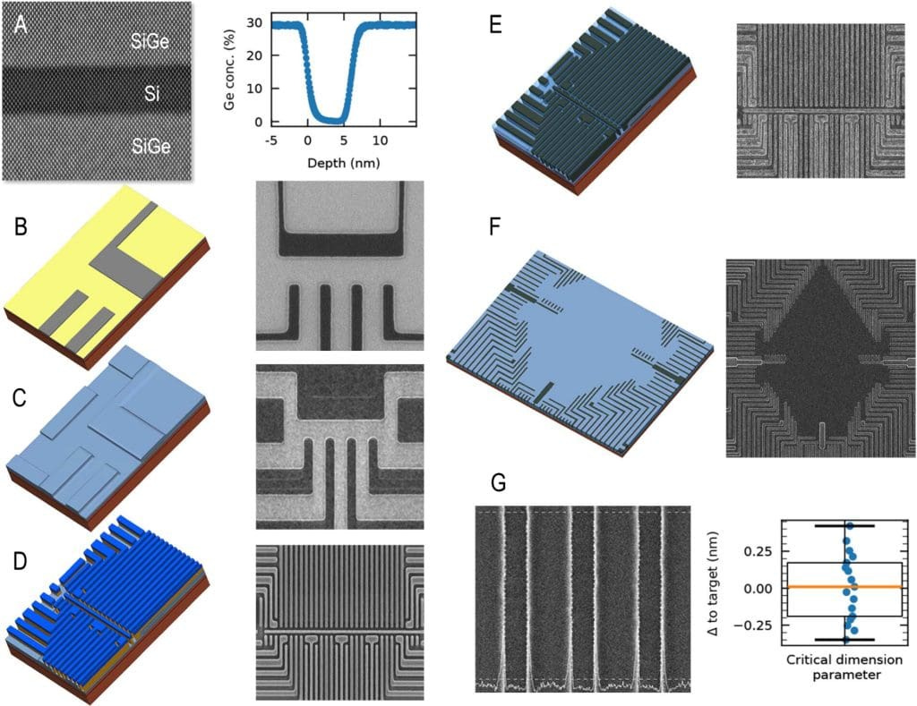
The Tunnel Falls test chip represents a crucial step towards scaling extensible 2D qubit array schemes. The device contains 12 quantum dot spin qubit linear arrays. They are fabricated using immersion and extreme ultraviolet lithography (EUV). These methods are combined with other standard high-volume manufacturing processes and production-level process control. This approach leverages industrial expertise and infrastructure to overcome the limitations of traditional quantum computing methods.
The Tunnel Falls test chip is a customized quantum test chip that provides an overview of the design, fabrication, and demonstration of a new spin-qubit platform. The device features key device characteristics, fabrication details, and qubit characterization results that confirm device functionality. These results corroborate the fabrication methods and are crucial for scaling extensible 2D qubit array schemes. Leveraging industrial expertise and infrastructure helps researchers overcome the limitations of traditional quantum computing methods and develop more scalable and practical approaches to quantum computing.
Intel’s approach to developing a practical quantum computer differs significantly from traditional methods. Most spin qubit devices are fabricated using a combination of EBL and liftoff processes. However, Intel’s method leverages immersion and EUV lithography. It also uses other standard high-volume manufacturing processes and production-level process control.

Intel’s approach differs from other alternative methods that employ modified fin and planar-based CMOS devices. While these methods offer improved scalability and reproducibility, they may not be as scalable or practical as Intel’s method.
The Tunnel Falls test chip features several key characteristics, including:
12 quantum dot spin qubit linear arrays
Fabrication using immersion and EUV lithography along with other standard high-volume manufacturing processes as well as production-level process control
Qubit characterization results confirming device functionality
These features represent a significant achievement in the field of quantum computing. By leveraging industrial expertise and infrastructure, researchers can overcome the limitations of traditional quantum computing methods. They can develop more scalable and practical approaches to quantum computing.
The development of Tunnel Falls represents a crucial step towards scaling extensible 2D qubit array schemes. However, much work remains to be done to develop practical quantum computers.
Publication details: “12-Spin-Qubit Arrays Fabricated on a 300 mm Semiconductor Manufacturing Line”
Publication Date: 2024-12-25
Authors: Hubert C. George, Mateusz Mądzik, Eric Henry, Andrew Wagner, et al.
Source: Nano Letters
DOI: https://doi.org/10.1021/acs.nanolett.4c05205


What are the coherence times and 1Q and 2Q fidelities?